 | –≠–ª–µ–∫—Ç—Ä–æ–Ω–Ω—ã–π –∫–æ–º–ø–æ–Ω–µ–Ω—Ç: STV0676 | –°–∫–∞—á–∞—Ç—å:  PDF PDF  ZIP ZIP |
October 2002
ADCS 7280926C
1/21
STV0676
CMOS Digital Camera Co-processor
Æ
The STV0676 co-processor combined with ST
CMOS image sensors offers highly integrated
imaging products which deliver USB 1.1, RGB-
preview, YCrCb or M-JPEG digital video data at up
to 30 frames per second.
The STV0676 interfaces to CIF (352 x 288) or VGA
(640 x 480) image sensor and performs:
- pixel defect correction,
- auto exposure, auto gain,
- auto white balance, anti-aliasing, anti-flicker,
- colour interpolation, colour balance,
- gamma correction,
- M-JPEG compression.
STV0676 chipsets are supported by a fully-featured
USB driver. This provides a wide range of user
definable settings for optimum camera setup and
operation. Isochronous data transfer over USB
guarantees video quality at all times, irrespective of
the number of other peripherals.
Low power consumption, highly integrated designs
and simple support circuitry enable OEMs to design
low cost, low power, camera products for high
volume consumer market places.
STMicroelectronics offers camera manufacturers
rapid-to-market camera products supported by
comprehensive reference designs, software drivers
and technical backup.
KEY FEATURES
s
Real-time video - up to 30fps VGA
s
USB 1.1 compliant
s
Motion-JPEG compression
s
Isochronous USB data transfer
s
Direct Show driver support
s
Programmable vendor ID
s
RGB-preview, YCrCb or M-JPEG video output
s
Automatic exposure, gain and white balance
APPLICATIONS
USB camera:
- Biometric identification, toys and games
Embedded applications support:
- PDA, notebook PC, mobile phone
- Set top box, and security applications
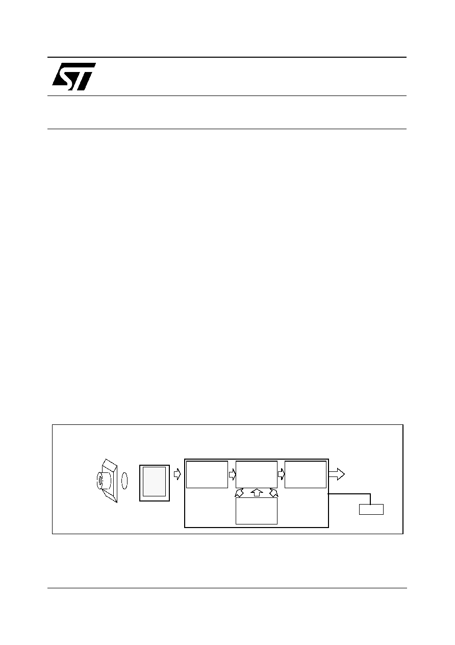
Typical application
CMOS Sensor
CIF or VGA
lens + IR filter
to host PC
USB Cable
STV0676
EEPROM
image
array
MIcro
Processor
USB
Interface
Video
Compression
Video
Processor

STV0676
2/21
Table of contents
Chapter 1
Overview . . . . . . . . . . . . . . . . . . . . . . . . . . . . . . . . . . . . . . . . . . . . . . . . . . . . . . . . .5
1.1
STV0676 co-processor general description ......................................................................... 5
1.2
Video processor (VP) ........................................................................................................... 5
1.2.1
Sensor interface ................................................................................................... 5
1.2.2
Video processor functions .................................................................................... 6
1.3
Auto exposure and gain control ........................................................................................... 7
1.4
Defect correction .................................................................................................................. 7
1.5
Video compression (VC) engine .......................................................................................... 7
1.6
Control processor ................................................................................................................. 7
1.7
Power management ........................................................................................................... .. 7
Chapter 2
External interfaces . . . . . . . . . . . . . . . . . . . . . . . . . . . . . . . . . . . . . . . . . . . . . . . . .8
2.1
USB interface ....................................................................................................................... 8
2.2
Mode selection ..................................................................................................................... 9
2.3
Selecting VID and PID via the digiport ................................................................................. 9
2.4
Serial EEPROM ................................................................................................................. 10
2.4.1
EEPROM format and contents ........................................................................... 11
2.4.2
Strings ................................................................................................................ 11
2.4.3
CheckSum ......................................................................................................... 12
2.5
I2C slave mode .................................................................................................................. 12
2.6
Digiport ............................................................................................................................... 12
2.7
General purpose input and output ...................................................................................... 12
Chapter 3
STV0676 application example . . . . . . . . . . . . . . . . . . . . . . . . . . . . . . . . . . . . . . .13
3.1
USB webcam ..................................................................................................................... 13
3.2
Embedded camera ............................................................................................................. 13
Chapter 4
Detailed specifications . . . . . . . . . . . . . . . . . . . . . . . . . . . . . . . . . . . . . . . . . . . .14
4.1
STV0676 absolute maximum ratings ................................................................................. 14
4.2
STV0676 AC/DC characteristic .......................................................................................... 14
Chapter 5
Pinout and pin descriptions . . . . . . . . . . . . . . . . . . . . . . . . . . . . . . . . . . . . . . . .15
5.1
STV0676 pin details ........................................................................................................... 15

3/21
STV0676
Chapter 6
Package Details STV0676 64pin TQFP . . . . . . . . . . . . . . . . . . . . . . . . . . . . . . . .19
Chapter 7
Reference design and evaluation kits (RDK's and EVK's) . . . . . . . . . . . . . . . .20
Chapter 8
Ordering details . . . . . . . . . . . . . . . . . . . . . . . . . . . . . . . . . . . . . . . . . . . . . . . . . .20
Chapter 9
Design issues . . . . . . . . . . . . . . . . . . . . . . . . . . . . . . . . . . . . . . . . . . . . . . . . . . . .20
STV0676
4/21
Revision C
Document revision history
Table 1 : Document revision history
Revision
Date
Comments
1.0
17/01/01
First Product preview release
1.1
22/01/01
Information added on
- Microport
- Serial EEPROM
- digiport
- Slave I
2
C implementation
- I
2
C Register map
1.2
01/02/01
Microport description updated
A
07/03/01
Details of existing STV0672 register map removed
Added reference to VV6411 sensor
B
10/10/01
Document reformatted with ST template
C
13/08/02
Change from a chipset datasheet to co-processor only.
Update of driver reference and ordering details.

5/21
STV0676
Overview
1
Overview
1.1
STV0676 co-processor general description
The STV0676 is a digital video processor requiring no external RAM and a minimum of passive
support components to provide a complete USB camera. STV0676 accepts raw digital video data
from a ST VGA or CIF format CMOS sensor and is capable of transferring the resulting JPEG data
to a host PC over USB at rates up to 30 frames per second VGA.
The internal STV0676 architecture consists of a number of separate functional blocks:
q
Video processor (VP)
q
Video compressor (VC)
q
USB control block
q
General purpose controller
The VP controls the sensor and processes the raw RGB pixel data into YCbCr images.
This YCbCr data is compressed by the VC.
The USB control block transfers the compressed data to the host PC.
1.2
Video processor (VP)
1.2.1
Sensor interface
The VP interfaces directly to the image sensor. The sensor interface comprises:
q
5-wire data bus SDATA[4:0] for receiving both video data and embedded timing references,
q
2-wire serial control interface (SSDA, SSCL),
q
sensor clock SCLK
q
reset circuitry
q
sensor suspend control
Overview
STV0676
6/21
Revision C
1.2.2
Video processor functions
STV0676 provides a master clock SCLK to the camera module. Each 10-bit pixel value generated
by the sensor is transmitted across the 5 wire databus SDATA[4:0] as a pair of sequential 5-bit
nibbles, most significant nibble first. Codes representing the start and end frames and the start and
end of lines are embedded within the video data stream to allow the video processor to synchronise
with the video data stream.
The video processing engine performs the following functions on incoming data:
q
full colour restoration at each pixel site from Bayer-patterned input data,
q
matrixing/gain on each colour channel for colour purity,
q
peaking for image clarity,
q
gamma correction,
q
colour space conversion from raw RGB to YCbCr[4:2:2].
The 2-wire sensor serial interface (SSDA and SSCL) provides control of sensor configuration.
Note:
the MSBit SDATA5 of the databus is unused in the current application but it will support future
sensors where a 12bit ADC architecture may be used.
Figure 1: Block diagram of STV0676 video processor module
Video Compression (VC) Engine
Video Processor
Stream
Digiport
D+
D-
Clocks
+ PLL
12MHz
XTAL
8052 Core
ROM
GPIO/mode
10
STV0676
RAM
Compressed Data
Control +
FIFOs
Ext.
Interrupts
CIF/VGA
Sensor
10
I
2
C Interface
USB core /glue
logic and
command FIFO's
General purpose
housekeeper functions
including AEC, AGC and
AWB
SDA
SCL
RESET
SDATA[4:0]
SSCL
SSDA
RESET_N
SCLK
SUSPEND
select
USB port

7/21
STV0676
Overview
1.3
Auto exposure and gain control
The STV0676 automatically controls the sensor exposure, which is evaluated (and, where
necessary modified) once per frame, where a frame consists of 2 video fields. The video fields are
identical in length, that is, they do not contain any of the half line detail of the analogue video
standards like CCIR or NTSC. Two fields per frame are required by the internal sensor video timing
model. Integration time, sensor analogue gain and STV0676 digital gain are all used to control the
overall exposure. The STV0676 exposure algorithm uses an asymptotic approach in calculating the
change required in the present exposure value to approach the requested exposure target.
1.4
Defect correction
STV0676 automatically detects and corrects pixel defects without the need for any additional
components or sensor calibration procedures. This greatly simplifies camera assembly and test
when compared with previous EEPROM-based defect correction schemes. The pixel defect
correction scheme ensures that the STV0676 + ST CMOS sensor appears as a `defect free'
chipset.
1.5
Video compression (VC) engine
The video compression engine performs 3 main functions:
q
up scaling of input YCbCr 4:2:2 video stream from the VP (typically to scale from QVGA to CIF
image formats),
q
compression and encoding of YCbCr stream into Motion-JPEG (M-JPEG) format,
q
USB bandwidth monitoring.
The data stream from the VP can be up to VGA size. The scaler in VC can downsize this image.
Once scaled the video stream is then converted into M-JPEG format. M-JPEG simply treats video
as a series of JPEG still images. The conversion is realised via a sequential DCT (discrete cosine
transform) with Huffman encoding. After transfer over USB, the M-JPEG stream is decoded in the
device driver running on the host.
The VC module is capable of compression ratios of up to 100:1 although this is scene-dependent.
Image framerate produced by the STV0676 chipset is fixed and furthermore the available USB
bandwidth is also fixed (within the software driver). The VC module varies the compression ratio to
match the fluctuating input video data rates to the available USB bandwidth and required framerate.
The final stage of the VC block manages the data transfer from the local VC FIFO store to the USB
core. STV0676 performs this management automatically by employing long-term (frame-level) and
short-term (block-level) compression management.
1.6
Control processor
The embedded 8052 microprocessor core controls the data flow through the major sub blocks
within STV0676 as well as the I
2
C communications to reconfigure the VP corresponding to requests
from the device driver.
1.7
Power management
The chipset conforms to all power requirements specified by USB Version 1.1.
External interfaces
STV0676
8/21
Revision C
2
External interfaces
2.1
USB interface
The USB interface is designed to be compliant with version 1.1 of the USB specification. The
STV0676 is a low power device and is therefore suitable for connection to any USB port on a PC,
self-powered hub or when connected to a bus-powered hub.
The device complies with the device framework specified in Chapter 9 of the USB specification as
follows:
q
The device supports a single high power configuration (
Configuration 1
).
q
Endpoint 0 is the default control endpoint and is always supported.
q
Endpoint 0 supports all of the USB commands required by the device framework.
q
Vendor specific commands on Endpoint 0 are used for all device control.
q
Configuration 1 supports a single interface (interface 0).
q
Interface 0 supports 8 alternate settings (alternates 0-7).
q
The alternate settings support between 0 and 2 additional endpoints.
q
Endpoint 1 is used for isochronous transfer of image data.
q
Endpoint 3 is used for transferring status information, e.g. state of a hardware button.
q
The endpoints are configured as follows (
Table 2
) in the alternate settings:
The best and most consistent performance in terms of image quality is always obtained in the
highest bandwidth setting (alternate 7). Under some circumstances it may not be possible for the
host to allocate this amount of USB bandwidth to the device.
The isochronous settings reserve varying quantities of bandwidth - from 10% to 85% of USB
bandwidth. The lower settings result in poor image quality due to heavy compression applied to
maintain a high framerate streaming of image data, but at the same time leaving more bandwidth
free for other USB devices. This is desirable if more than one camera is to be used, or if there are
other isochronous peripherals connected. The device driver allows the user to specify the maximum
bandwidth they wish to allocate to transfer data from the device. If the maximum specified by the
user is not available, perhaps because another isochronous device has already reserved that
bandwidth, then lower alternates are tried until one succeeds.
Table 2: Endpoint alternate settings
Alternate setting
Endpoint1 (isochronous)
Endpoint3 (interrupt)
0
Not present
Not present
1
Not present
8 bytes / packet; 1 packet /8 frames
2
128 bytes / packet; 1 packet / frame
8 bytes / packet; 1 packet /8 frames
3
384 bytes / packet; 1 packet / frame
8 bytes / packet; 1 packet /8 frames
4
640 bytes / packet; 1 packet / frame
8 bytes / packet; 1 packet /8 frames
5
768 bytes / packet; 1 packet / frame
8 bytes / packet; 1 packet /8 frames
6
896 bytes / packet; 1 packet / frame
8 bytes / packet; 1 packet /8 frames
7
1023 bytes / packet; 1 packet / frame
8 bytes / packet; 1 packet /8 frames
9/21
STV0676
External interfaces
Benchmark testing of the STV0676 indicates that 30fps CIF video (compressed) can be
accommodated in 50% of USB bandwidth.
2.2
Mode selection
All USB devices report a VID, PID and power consumption as part of a standard device descriptor.
The VID and PID for STV0676 can be configured by the state of the digiport bits or by using an
external EEPROM. The mode selection is made using the two MODESEL pins as described in
Table 3
below.
2.3
Selecting VID and PID via the digiport
Tables 4~7 demonstrate how the VID/PID information is defined via the digiport.
The current reference design for the STV0676-chipset has digiport[7:0] connected to VSS, thus the
VID and PID are 16'h0553 and 16'h0140 respectively.
The digiport also controls the device current consumption that is reported to the host at device
enumeration.
Table 3: Mode selection
MODESEL[1]
MODESEL[0]
Mode of operation
0
0
USB Mode. External EEPROM fitted, therefore PID, VID and power
consumption read from this source. See
Section 2.4
1
0
Slave I
2
C mode.
0
1
USB mode. Default. No external EEPROM fitted, the PID
VID and power consumption data determined by digiport[7:0].
See
Section 2.3
1
1
Reserved
Table 4: Basic digiport configuration
digiport bit slice
function
[3:0]
configures the LS nibble of the PID
[5:4]
master VID/PID select
[7:6]
power setting
Table 5: Digiport LS nibble configuration
digiport[3:0]
PID LS nibble
4'b0000
4'b0000
4'b0001
4'b0001
4'b0010
4'b0010
4'b0011
4'b0011
4'b0100
4'b0100
4'b0101
4'b0101
External interfaces
STV0676
10/21
Revision C
2.4
Serial EEPROM
STV0676 is designed to be used with a 128 or 256 byte serial I
2
C EEPROM. The EEPROM can be
programmed with data to allow a user to fully customise the USB identity of STV0676. The
configuration of this data is as follows.
4'b0110
4'b0110
4'b0111
4'b0111
4'b1000
4'b1000
4'b1001
4'b1001
4'b1010
4'b1010
4'b1011
4'b1011
4'b1100
4'b1100
4'b1101
4'b1101
4'b1110
4'b1110
4'b1111
4'b1111
Table 6: Master VID/PID selection
digiport[5:4]
VID/PID reported
2'b00
16'h0553/16'h014x
a
2'b01
16'h0553/16'h015x
a
2'b10
16'h0553/16'h026x
a
2'b11
16'h0553/16'h017x
a
a. The `x' ls nibble of the PID is defined by the value from
Table 5
above
Table 7: Device power consumption indicator
digiport[7:6]
current consumption reported
2'b00
98mA
2'b01
250mA
2'b10
350mA
2'b11
500mA
Table 5: Digiport LS nibble configuration
digiport[3:0]
PID LS nibble
11/21
STV0676
External interfaces
2.4.1
EEPROM format and contents
The remaining space is available for the string blocks indexed at locations 8, 9 and 10.
2.4.2
Strings
The strings referred to above (locations 8-10), are the USB string descriptors referenced from the
device, configuration and interface descriptors. The value should be set to '0' if the string is not
implemented or to the offset in bytes of the start of the string block in the EEPROM.
The first byte of each string block is the number of the characters in the string. Subsequent bytes
are the actual string, which need not include a terminating null (
Table 9
:).
Table 8: EEPROM format and contents
location
contents
0
fixed number, must be 0x'ED
1
fixed number, must be 0x'15
2
reserved, must be 0x'00
3
max device power (=mA/2, e.g. 400mA enter 0x'C8)
4
VidLo, low byte of the vendor ID
5
VidHi, highbyte of the vendor ID
6
PidLo, low byte of the product ID
7
PidHi, highbyte of the product ID
8
manufacturer string offset, example below
9
product string offset, see below
10
interface 0 String offset
11
reserved, must be 0x'00
12
reserved, must be 0x'00
13
checksum
Table 9: EEPROM device string example
Location
Contents
8
Manufacturer string offset = 16
16
String length = 5
17
String text = `H' (in ascii)
18
String text = `e' (in ascii)
19
String text = `l' (in ascii)
20
String text = `l' (in ascii)
21
String text = `o' (in ascii)

External interfaces
STV0676
12/21
Revision C
2.4.3
CheckSum
The checksum is calculated by adding the byte value of EEPROM locations 0 to 12 inclusive, the
low order byte of the result is stored in location 13.
2.5
I
2
C slave mode
STV0676 can be configured to behave as an I
2
C slave. This allows the device to be configured by
host devices other than PCs. Details of the I
2
C messages supported and description of the I
2
C
register bank are available from STMicroelectronics.
2.6
Digiport
The Digiport is a 10-bit bi-directional data port which can be used to transfer video data in or out of
the device. This port can also be used to configure USB descriptor information at power up see
(
Section 2.3
). Full details on the digiport operation and control are available from
STMicroelectronics.
2.7
General purpose input and output
STV0676 provides up to 8 pins which can be used as general purpose I/O. These pins can be used
to interface to led's, buzzers, switches etc.
13/21
STV0676
STV0676 application example
3
STV0676 application example
3.1
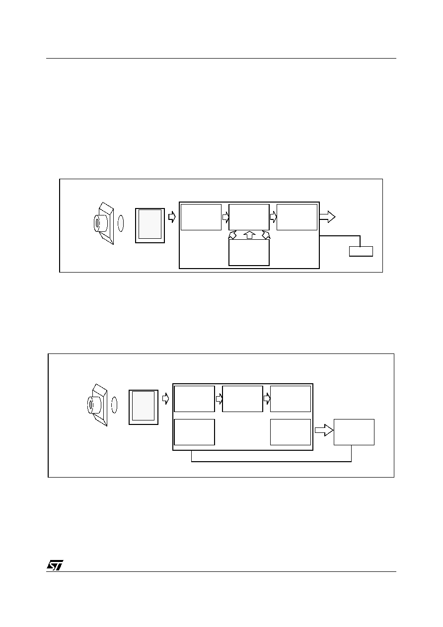
USB webcam
Figure 2
shows a block diagram of a basic webcam using the minimum of external components.
The camera is controlled entirely through PC drivers over USB.
Note:
If required a custom USB PID/VID can be configured by the use of an EEPROM, as detailed in
Section 2.3
3.2
Embedded camera
Figure 3
shows a block diagram of a camera intended for embedded applications, outputting JPEG,
YCrCb or RGB preview over an 8bit bus, the third party electronics would control the STV0676
using I
2
C.
Figure 2: Webcam block diagram
Figure 3: Embedded camera block diagram
CMOS Sensor
CIF or VGA
lens + IR filter
to host PC
USB Cable
STV0676
EEPROM
image
array
MIcro
Processor
USB
Interface
Video
Compression
Video
Processor
CMOS Sensor
CIF or VGA
lens + IR filter
STV0676
image
array
MIcro
Processor
FIFO
Video
Compression
Video
Processor
Digiport
Third party
electronics
I
2
C
Detailed specifications
STV0676
14/21
4
Detailed specifications
4.1
STV0676 absolute maximum ratings
4.2
STV0676 AC/DC characteristic
Description
Range
Unit
Operating Temperature
0 to 70
o
C
Storage Temperature
-50 to 150
o
C
Parameter
Description
Min
Typ
Max
Units
VDD_CORE
Primary STV0676 power supply
1.55
1.8
1.95
V
VDD_IO
3.3V power supply for on-chip USB transceiver and IO
3.0
3.3
3.6
V
VDD_PLL
Analog supply to the PLL
1.60
1.8
2.0
V
I_core
suspend
Current consumption in suspend mode
3
µA
I_core
standby
Current consumption in standby mode
9.6
mA
I_core
active
Current consumption while active, VGA 30fps
52
mA
I_IO
suspend
Current consumption in suspend mode
40
µA
I_IO
standby
Current consumption in standby mode
540
µA
I_IO
active
Current consumption while active, VGA 30fps
6.6
mA
I_PLL
suspend
Current consumption in suspend mode
0.4
µA
I_PLL
standby
Current consumption in standby mode
476
µA
I_PLL
active
Current consumption while active, VGA 30fps
476
µA
V
Il
CMOS input low voltage (XTAL_IN)
0.687
V
V
IH
CMOS input high voltage (XTAL_IN)
1.19
V
V
HYS
Hysteresis (XTAL_IN)
0.51
V
V
Il
CMOS input low voltage
0.35VDD
V
V
IH
CMOS input high voltage
0.65VDD
V
V
T+
CMOS schmitt input low to high threshold voltage
2.15
V
V
T-
CMOS schmitt input high to low threshold voltage
1.05
V
V
T
Threshold point
1.65
V
V
OH
Output high voltage
2.4
V
V
OL
Output low voltage
0.4
V
15/21
STV0676
Pinout and pin descriptions
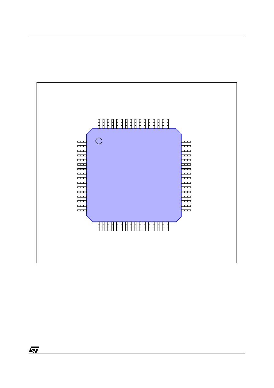
5
Pinout and pin descriptions
5.1
STV0676 pin details
Figure 4: STV0676 pinout
IO_VDD
SW0_N
IO_
V
D
D
CORE_V
SS
TEST_CONF[1]
USB
_
DP
EE
PRO
M
_
S
DA
EE
PRO
M
_
S
CL
USB
_
DN
PLL_VDD
PLL_VSS
XTAL_IN
XTAL_OUT
CORE_VSS
IO_VDD
IO_VSS
DIGIPORT[9]
RESET_N
GPIO[7]
IO_VSS
R
E
SE
R
V
ED
[2]
SW1_N
SSDA
SSCL
IO_
V
S
S
DIGIPORT[5]
CORE_VDD
TEST_CONF[0]
TEST_CONF[2]
SPDN
CORE
_VDD
M
O
D
ESE
L
[
1]
IO_V
S
S
RE
SE
R
V
ED[
0
]
M
O
D
E
SE
L[
0]
DIGIPORT[7]
DIGIPORT[8]
DIGIPORT[6]
R
E
SE
R
V
ED
[4]
R
E
SE
R
V
ED
[3]
RE
SER
V
E
D[
1
]
DIGIP
OR
T
[
4]
DI
GI
P
O
R
T
[
3
]
DIGIP
OR
T
[
2]
DIGIP
OR
T
[
1]
DI
GI
P
O
R
T
[
0
]
IO_V
D
D
IO_V
S
S
CORE
_VDD
CO
R
E
_
V
SS
S
E
NS
OR_CLK
S
E
N
S
OR_DB
[
5]
S
E
N
S
OR_DB
[
4]
S
E
N
S
OR_DB
[
3]
S
E
N
S
OR_DB
[
2]
S
E
N
S
OR_DB
[
1]
S
E
N
S
OR_DB
[
0]
1
17
16
32
33
48
49
64
GPIO[6]
GPIO[5]
GPIO[4]
GPIO[3]
GPIO[2]
GPIO[1]
GPIO[0]

Pinout and pin descriptions
STV0676
16/21
Table 10: STV0676 pin description
Pin
Signal
Type
Description
POWER SUPPLIES
4
PLL_VDD
INPUT
VDD for internal phase locked loop
5
PLL_VSS
INPUT
GND for internal phase locked loop
8
CORE_VDD
INPUT
VDD for core logic
9
CORE_VSS
INPUT
Ground for core logic
10
IO_VDD
INPUT
VDD for pad ring
11
IO_VSS
INPUT
Ground for pad ring
22
IO_VDD
INPUT
VDD for pad ring
23
IO_VSS
INPUT
Ground for pad ring
24
CORE_VDD
INPUT
VDD for core logic
25
CORE_VSS
INPUT
Ground for core logic
39
IO_VDD
INPUT
VDD for pad ring
40
IO_VSS
INPUT
Ground for pad ring
49
IO_VSS
INPUT
Ground for pad ring
57
IO_VDD
INPUT
VDD for pad ring
58
IO_VSS
INPUT
Ground for pad ring
59
CORE_VDD
INPUT
VDD for core logic
60
CORE_VSS
INPUT
Ground for core logic
DEVICE MASTER CLOCK AND RESET
6
XTAL_IN
ANA
System clock pad
7
XTAL_OUT
OSC
System clock pad
33
RESET_N
SCHMITT
System, power-on-reset supplied by companion sensor
DIGIPORT/USB CONFIGURATION INTERFACE
12
DIGIPORT[9]
BIDIR
Digiport operation
13
DIGIPORT[8]
BIDIR
Digiport operation
14
DIGIPORT[7]
BIDIR
Digiport operation /programmable USB current consumption reported
15
DIGIPORT[6]
BIDIR
Digiport operation /programmable USB current consumption reported
16
DIGIPORT[5]
BIDIR
Digiport operation /programmable USB VID/PID
17
DIGIPORT[4]
BIDIR
Digiport operation /programmable USB VID/PID
18
DIGIPORT[3]
BIDIR
Digiport operation /programmable USB PID
19
DIGIPORT[2]
BIDIR
Digiport operation /programmable USB PID
20
DIGIPORT[1]
BIDIR
Digiport operation /programmable USB PID
21
DIGIPORT[0]
BIDIR
Digiport operation /programmable USB PID
SENSOR INTERFACE
26
SENSOR_CLK
BIDIR
Sensor clock
17/21
STV0676
Pinout and pin descriptions
27
SENSOR_DB[5]
INPUT
Sensor data bus [bit5]
28
SENSOR_DB[4]
INPUT
Sensor data bus [bit4]
29
SENSOR_DB[3]
INPUT
Sensor data bus [bit3]
30
SENSOR_DB[2]
INPUT
Sensor data bus [bit2]
31
SENSOR_DB[1]
INPUT
Sensor data bus [bit1]
32
SENSOR_DB[0]
INPUT
Sensor data bus [bit0]
34
SSDA
3 state
Sensor serial interface data
35
SSCL
3 state
Sensor serial interface clock
36
SPDN
BIDIR
Control line to sensor to select ultra low power SUSPEND mode
MISC CONTROL
37
SW1 _N
INPUT
Spare switch input
38
SW0 _N
INPUT
Remote wakeup
GPIO INTERFACE/ OTHER
41
GPIO[0]
BIDIR
General purpose input/output (GPIO)
42
GPIO[1]
BIDIR
General purpose input/output (GPIO)
43
GPIO[2]
BIDIR
General purpose input/output (GPIO)
44
GPIO[3]
BIDIR
General purpose input/output (GPIO)
45
GPIO[4]
BIDIR
General purpose input/output (GPIO)
46
GPIO[5]
BIDIR
General purpose input/output (GPIO)
47
GPIO[6]
BIDIR
General purpose input/output (GPIO)
48
GPIO[7]
BIDIR
General purpose input/output (GPIO)
50
MODESEL[0]
BIDIR
Along with ModeSel[1] used to configure I
2
C interface and PID/VID
selection. Please see
Table 3
for further details
51
RESERVED[0]
BIDIR
Not connect in reference design
52
RESERVED[1]
BIDIR
Connect to VDD in reference design
53
MODESEL[1]
BIDIR
Along with ModeSel[0] used to configure I
2
C interface and PID/VID
selection. Please see
Table 3
for further details
54
RESERVED[2]
BIDIR
Connect to VDD in reference design
55
RESERVED[3]
BIDIR
Not connect in reference design
56
RESERVED[4]
BIDIR
Not connect in reference design
Table 10: STV0676 pin description
Pin
Signal
Type
Description
Pinout and pin descriptions
STV0676
18/21
USB INTERFACE
61
USB_DN
BIDIR
USB data line
62
USB_DP
BIDIR
USB data line
TEST MODE SELECTION
1
TEST_CONF[0]
INPUT
Test configuration bit - connect to VDD for normal operation
2
TEST_CONF[1]
INPUT
Test configuration bit - connect to VDD for normal operation
3
TEST_CONF[2]
INPUT
Test configuration bit - connect to VDD for normal operation
EEPROM INTERFACE
a
63
EEPROM_SDA
BIDIR
Serial data to/from the EEPROM or slave I
2
C clock
64
EEPROM_SCL
BIDIR
Serial clock to the EEPROM or slave I
2
C clock
a. The I
2
C pins EEPROM_SCL and EEPROM_SDA can be reconfigured to act as a low speed I
2
C
slave device that allows the user to directly control the internal register space of the VP and VC
modules.
Table 10: STV0676 pin description
Pin
Signal
Type
Description
19/21
STV0676
Package Details STV0676 64pin TQFP
6
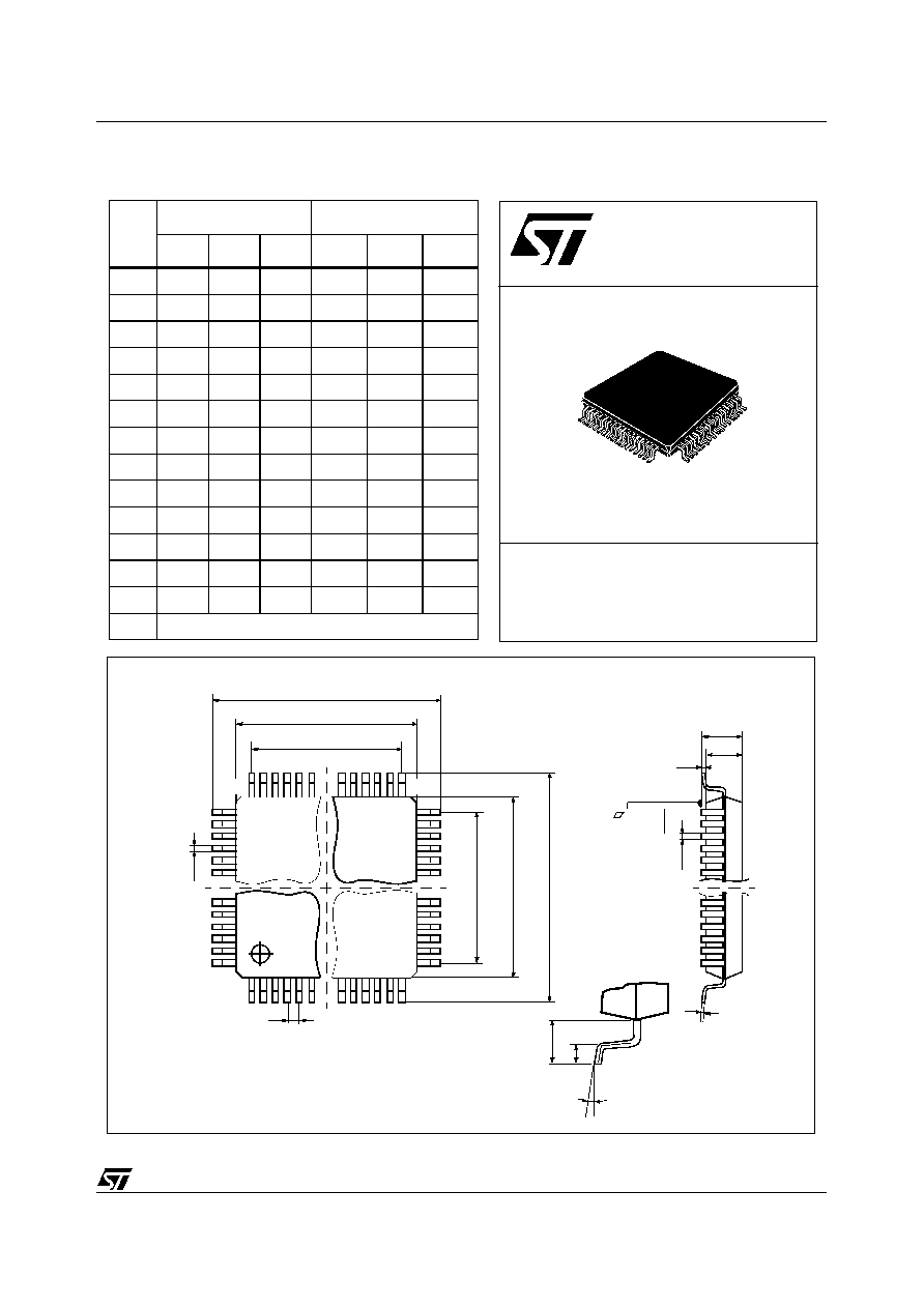
Package Details STV0676 64pin TQFP
Dim.
mm
inch
Min
Typ
Max
Min
Typ
Max
A
1.60
0.063
A1
0.05
0.15
0.002
0.006
A2
1.35
1.40
1.45
0.053
0.055
0.057
B
0.18
0.23
0.28
0.007
0.009
0.011
C
0.12
0.16
0.20
0.0047
0.0063
0.0079
D
12.00
0.472
D1
10.00
0.394
D3
7.50
0.295
e
0.50
0.0197
E
12.00
0.472
E3
7.50
0.295
L
0.40
0.60
0.75
0.0157
0.0236
0.0295
L1
1.00
0.0393
K
0∞C (min.), 7∞C (max.)
Weight: 0.30 gr
Body: 10x10x1.40mm
TQFP64
Æ
OUTLINE AND
MECHANICAL DATA
A
A2
A1
B
C
16
17
32
33
48
49
64
E3
D3
E1
E
D1
D
e
1
K
B
TQFP64
L
L1
Seating Plane
0.10mm

Reference design and evaluation kits (RDK's and EVK's)
STV0676
20/21
Revision C
ADCS 7280926
7
Reference design and evaluation kits (RDK's and EVK's)
STMicroelectronics supply a full range of supporting reference design kits for their range of sensors
and coprocessors.
Please refer to the STMicroelectronics website (Imaging Products under the quick links) for the up-
to-date list of available reference designs and evaluation kits.
8
Ordering details
For more information on the appropriate sensor choice please contact STMicroelectronics or refer
to the STMicroelectronics website (Imaging Products under the quick links).
9
Design issues
There are no restrictions on the positioning of the STV0676 coprocessor with respect to the sensor.
An EEPROM is required for full USB 1.1 compliance, see reference design manual for details.

ADCS 7280926
Revision C
21/21
STV0676
Information furnished is believed to be accurate and reliable. However, STMicroelectronics assumes no responsibility for the consequences
of use of such information nor for any infringement of patents or other rights of third parties which may result from its use. No license is
granted by implication or otherwise under any patent or patent rights of STMicroelectronics. Specifications mentioned in this publication are
subject to change without notice. This publication supersedes and replaces all information previously supplied. STMicroelectronics products
are not authorized for use as critical components in life support devices or systems without express written approval of STMicroelectronics.
The ST logo is a registered trademark of STMicroelectronics
Purchase of I
2
C Components by STMicroelectronics conveys a license under the Phillips I
2
C Patent. Rights to use these
components in an I
2
C system is granted provided that the system conforms to the I
2
C Standard Specification
as defined by Phillips.
© 2002 STMicroelectronics - All Rights Reserved
STMicroelectronics GROUP OF COMPANIES
Australia - Brazil - China - Finland - France - Germany - Hong Kong - India - Italy - Japan
Malaysia - Malta - Morocco - Singapore - Spain - Sweden - Switzerland - United Kingdom - U.S.A.
http://www.st.com